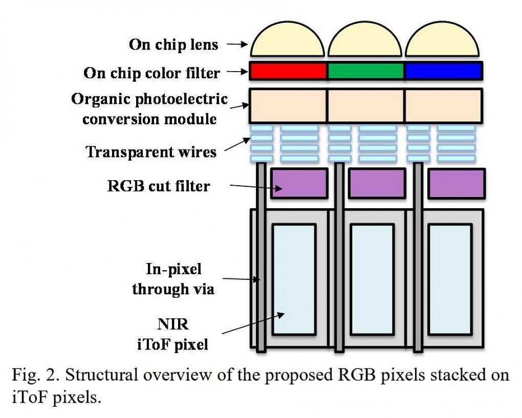
At the IEDM 2024 semiconductor trade fair, Sony Semicon presented a combination sensor in which the camera sensor is located directly above the depth sensor / Time-of-Flight sensor. This is made possible by the use of a new material: normally the color pixels would be located on silicon, but the broadband light would be absorbed and thus the depth pixels covered. However, Sony has apparently solved this problem by means of a new construction on a broadband transparent, organic photo-leading film. Visible wavelength hits the color sensors, while infrared light falls further down on the IR pixels of the ToF sensor. Above each ToF pixel, which each occupies 4µm, there are four RGB pixels with 1µm each. In total, there is talk of a resolution of 1004×756 pixels for the depth map and 4016×3024 pixels for the color image. At least in this respect, the prototype has apparently already reached a usable area.